
Dancing with electrons to light up the nanoscale
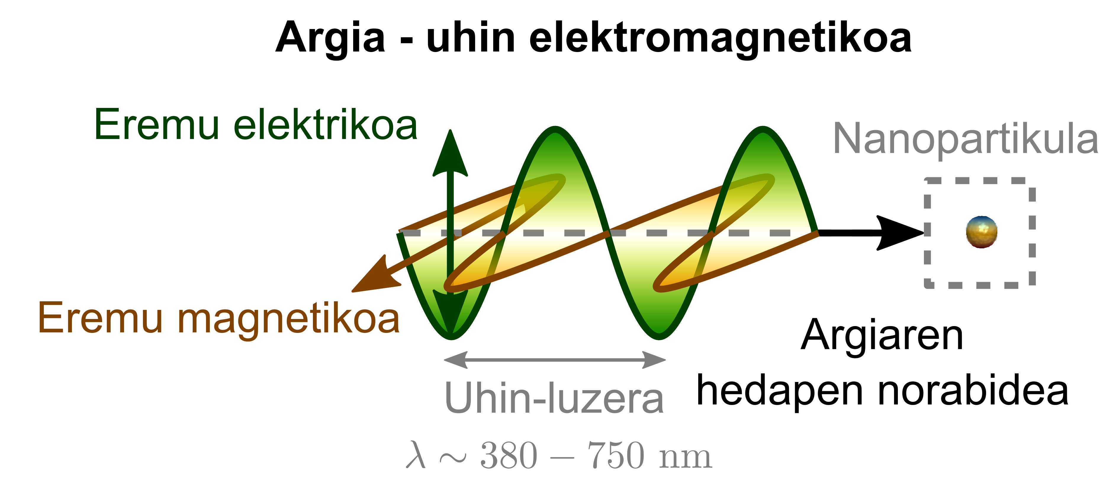
Many of the technological advances and scientific discoveries made throughout history have been based on improving our visual ability. XVI. and XVII. For centuries, inventions of magnifying glass, and especially early microscopes, gave a remarkable boost to biology and medicine. These traditional optical systems, however, have a limited resolution, that is, they support a diffraction that allows to characterize those details that have a light wave size similar to or greater than the wavelength of the light used. The wavelength is the twine wavelength, as shown in Figure 1. In the case of sea waves, for example, the distance between summits is usually about tens of metres. In the case of visible light, on the contrary, the wavelength oscillates between 380 nm and 750 nm, so it is not possible to distinguish smaller details using traditional optical systems.
To overcome the limit imposed by diffraction, we need techniques that allow us to confine light to a space that is less than its wavelength. Fortunately, the interaction of light and matter on the nanoscale can lead to the localization of light on this scale. To do this, we have to immerse ourselves in the realm of nanophotonics.
Dancing with electrons
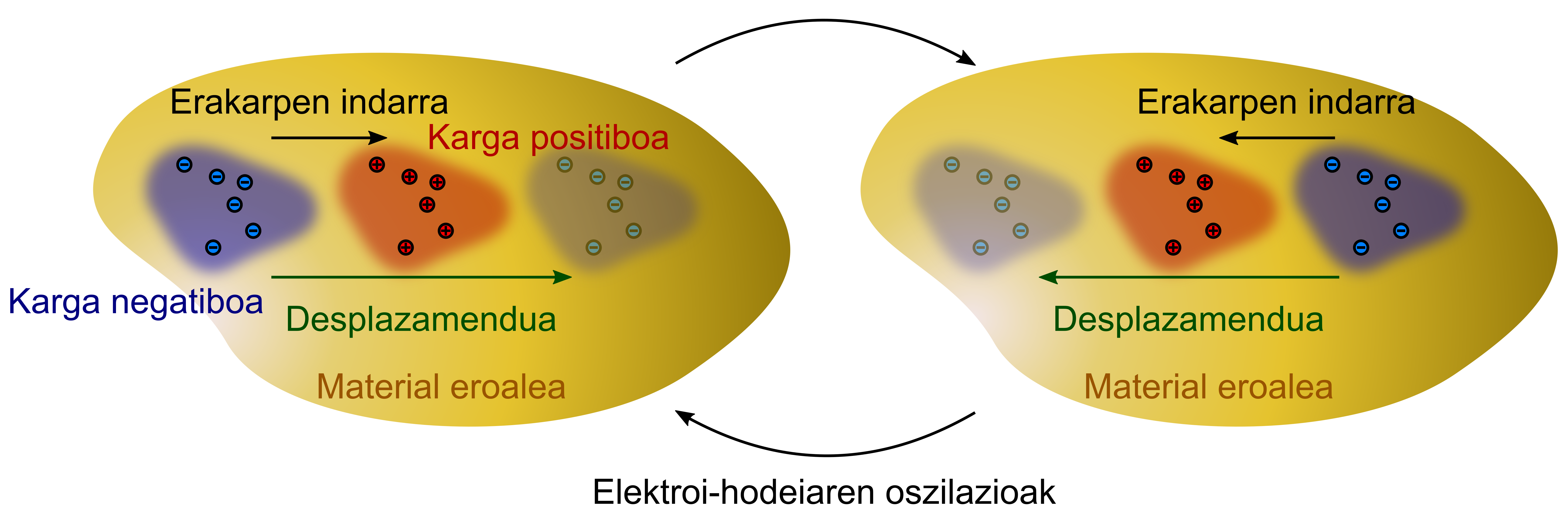
The confinement underlying the wavelength of light can be achieved, inter alia, by means of surface plasmons. What are plasmons? In conductive materials, unlike insulators, electrons can move freely. The set of free electrons can be represented as a gas or a cloud. If this cloud leaves its state of equilibrium —2. as shown in the figure, lack of electrons where it was at the beginning. At one point we will therefore have a surplus of negative charge and, at the same time, a positive overload in the region where these electrons were located. Due to the attraction of positive and negative charges to each other, the cloud-electron will withstand a force of attraction that will oscillate from one side to the other with its own frequency. That is, electrons can dance in conductive materials, and for that they have their own rhythm that depends on the material. These collective free electron oscillations are called plasmois.
Plasmons can be excised by light and, in general, by electromagnetic waves. In a closed and conductive structure such as a nanoparticle, local electrons will follow the electrical field of that wave and accumulate on one side of the surface of the nanoparticle, as shown in Figure 3. As the electric field of light oscillates, the electron-cloud will also oscillate following it, dancing to the rhythm that marks the light. If the frequency of light is equal to the natural frequency, we will have a resonance in the nanoparticle, that is, we will excite a plasmon.
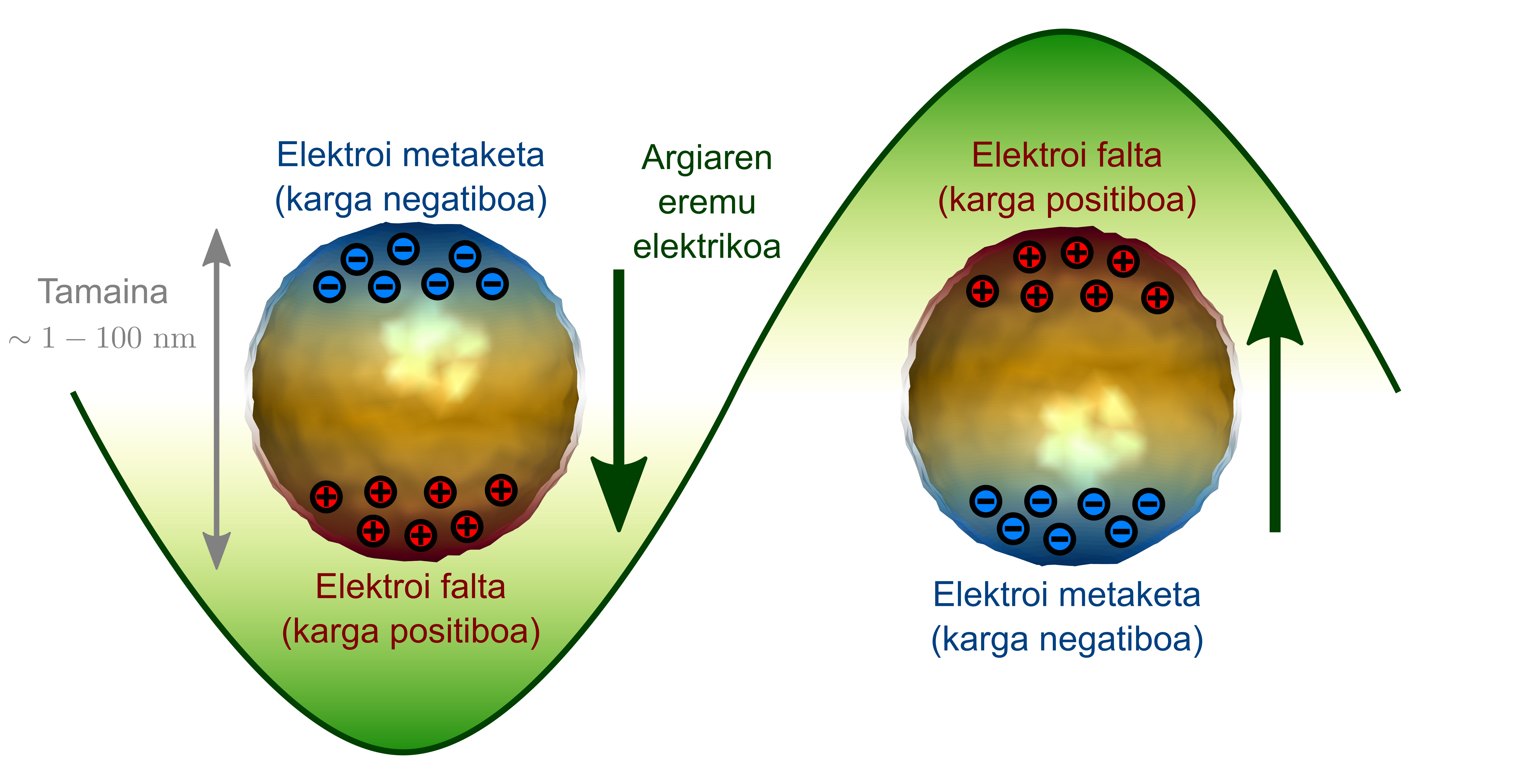
An accumulation of loads we have on the surface will generate an electric field called the induced area. This induced electric field is very violent around the surface where the load has been deposited. The intensity of illuminated light can be up to 100 times more intense than what we have used, but it weakens very quickly (exponentially) as we move away from the surface. This allows us to extend the field in a region of a few nanometers. Consequently, plasmons have the ability to locate light and can be used to exceed the diffraction limit. This allows us to differentiate details close to the surface of the nanoparticle, like molecules. Who would think that some electron dancers could clear up the nanoscale!
Not only that, plasma nanoparticles have the ability to locate light on the nanoscale, but also to disperse light at a distance. That is, as an antenna, they have the ability to receive and then emit electromagnetic waves: they are nanoantennae. This ability allows us to interrogate plasma nanoparticles using light to get information about the nanoparticle and its environment.
Locating light to the limit
Excitable plasmons on nanoparticles are dependent on four characteristics: size, geometry, material and medium. In my thesis I have studied the influence of nanoparticles geometry on induced fields. In fact, around the vertices, the electric field is further located in the conductors, as more electrons accumulate there. This phenomenon is called the lightning rod effect (the function of lightning arrests is based on this phenomenon).
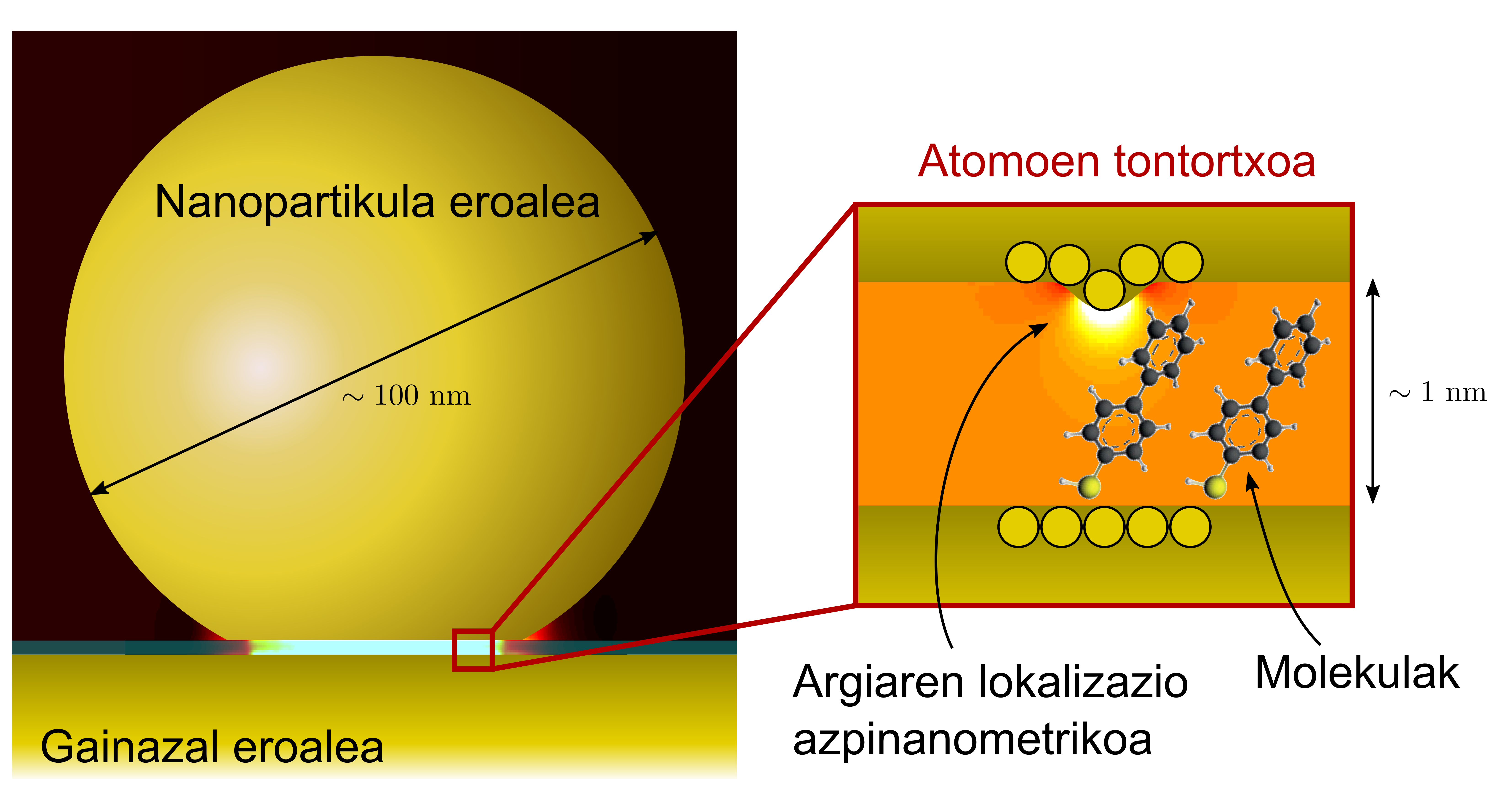
I've seen in my thesis that the behavior of electrons at atomic scale is similar. Its combination with plasmons allows the subanometric location of light. This subanometric location of light provides information about a very small space, as shown in Figure 4. For example, if we have molecules between nanoparticles and conductive surfaces, we can excite the vibrations of the latter and study their structure. Yes, molecules can dance too!
Elements needed to predict the location of light
To predict, by means of simulation, the location of the field that we can obtain in the vertices of a nanoparticle or nanostructure of these characteristics, we can use different models. In fact, we should start from a model that takes into account the position of atoms, that is, the crystalline structure. Not only that, but also the quantum character of electrons. However, in this thesis we have used simpler models to predict the location of the field and the size of the expansion. The form or form of the electron cloud-without external excitation, i.e., without lighting, can be sufficient in many cases. Figure 5 shows two examples. In other words, it is not essential to describe in detail the crystalline structure. The parties room has been placed with walls, taking into account the space the electrons use to dance, so that the rhythm of music and the movements of the dancers do not undergo significant changes.

Instead of using light to analyze samples and excite plasmons, we can use other techniques. Electrodes can be used, for example, using scanning and transmission electronic microscopes. This type of microscopes release electron-beam to collect samples after colliding or crossing them. In this way, parameters such as the energy lost by the generators, the deviation they have suffered, are measured. These data allow analyzing the properties of the sample. In addition, a far better resolution than with light is achieved and a resolution below nanometers is allowed. Electrodes can also be used to excite plasmons in conductive nanostructures. By their resolution, the electrodes are more sensitive than the techniques that use light on the geometry of the nanoparticle. A unique opportunity to define the limits of models. As I have demonstrated in my thesis, the detailed description of the geometry of the nanoparticle in the simple models mentioned is essential to confirm the results obtained in more complex models.
The more or less approximated appreciation of the geometry facilitates the simulations considerably. Moreover, many of the nanostructures used in many experiments are too large and complex to be able to consider atoms one by one and thus perform computer simulations. Simply, current computers do not have enough power to perform such heavy simulations. It is therefore necessary to determine the limitations and capabilities of the simplest models available to confirm the reliability of the results and forecasts obtained in the simulations. We don't have to give him when it comes to dancing with the missing electrons.
BIBLIOGRAPHY
L. Novotny and B. Hecht, “Principles of Nano-Optics”, Cambridge University Press, Cambridge, 2012.
P. N. Prasad, “Nanophotonics”, John Wiley & Sons, Inc., Hoboken, NJ, 2004.
M. Pelton, J. Aizpurua and G. Bryant, “Metal-nanoparticle plasmonics”, Laser & Photonics Review 2, 136–159 (2008).
F. Benz, M. C. Schmidt, A. Dreismann, R. Chikkaraddy, Y. Zhang, A. Demetriadou, C. Carnegie, H. Ohadi, B. de Nijs, R. Stephen, J. Aizpurua and J. J. Baumberg, “Single-molecule optomechanics in “picocavities”, Science 354, 726–729 (2016).
M. Urbieta, M. Barbry, Y. Zhang, P. Koval, D. Sánchez - Portal, N. Zabala and J. Aizpurua, “Trailers-Scale Lightning Rod Effect in Plasmonic Picocavities: A Classical View to a Quantum Effect”, ACS Nano 12, 585–595 (2018)
R. Egerton, “Electron Energy -Loss Spectroscopy in the Electron Microscope”. Springer US, Boston, MA, 2011.
F. J. García De Abajo, “Optical excitations in electron microscopy”, Reviews of Modern Physics 82, 209–275 (2010).
Zu idazle
Zientzia aldizkaria