

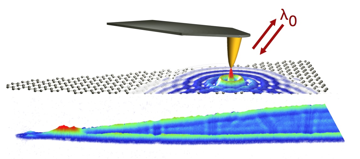
Light trapped on graphene surface
Light instead of electric current. This is one of the options that have been proposed to improve current microelectronics. Light is faster than electrons, but with no electric charge, it is difficult to control it electrically. A group of physicists from DIPC, CFM, Grafenea and CICNanoGUNE, together with physicists from ICFO of Barcelona and IQFR of Madrid, have faced this challenge in Gipuzkoa. The results have been published today by the journal Nature. Physicists have used graphene material to trap infrared light in a structure called plasmoi and control it freely.
“It’s a mixture of electrons and light,” explains Ralph Hillenbrand, principal investigator of this work. Light has size limits. The waves of a certain type of light have a certain length and it is not possible to control them by optical procedures with an accuracy greater than half of that wavelength.
But for this, the ray of light that you want to control must become something else, a plasmon. Physicists drive the beam to a surface and create a link with their electrons. They say that interaction is collective. And this interaction behaves like a wave. Light is trapped in that wave of electrons. It is a project. In addition, the application of a potential difference to the surface allows to introduce more or less electrons to the plasmon and manipulates its wavelength, amplitude and position. “The wavelength can be electrically reduced. That is very interesting. We can make the wavelength 40 times smaller,” says Hillenbrand. They have departed from infrared light, which has a wavelength of the size of the micron, and have created the plasmoia of some nanometers.
However, any surface is not valid. Gipuzkoa physicists have used graphene, a material that is lately fashionable in many areas of physics. It consists of layers of carbon atoms of a single atom of thickness and its electrons are arranged in the form of a gas cloud in two dimensions. “For this two-dimensionality, for example, electrons do not act as on the surface of a metal. It allows you to provoke any mischief.”
Through this technique they can capture, reduce and, if desired, eliminate the luminous wave. This way you can build a switch that, changing the potential difference, can simulate the behavior of a transistor. Light from plasmon can then be emitted, for example, for light to advance in an optical circuit. Therefore, currently graphene components are the best integration option in these circuits.
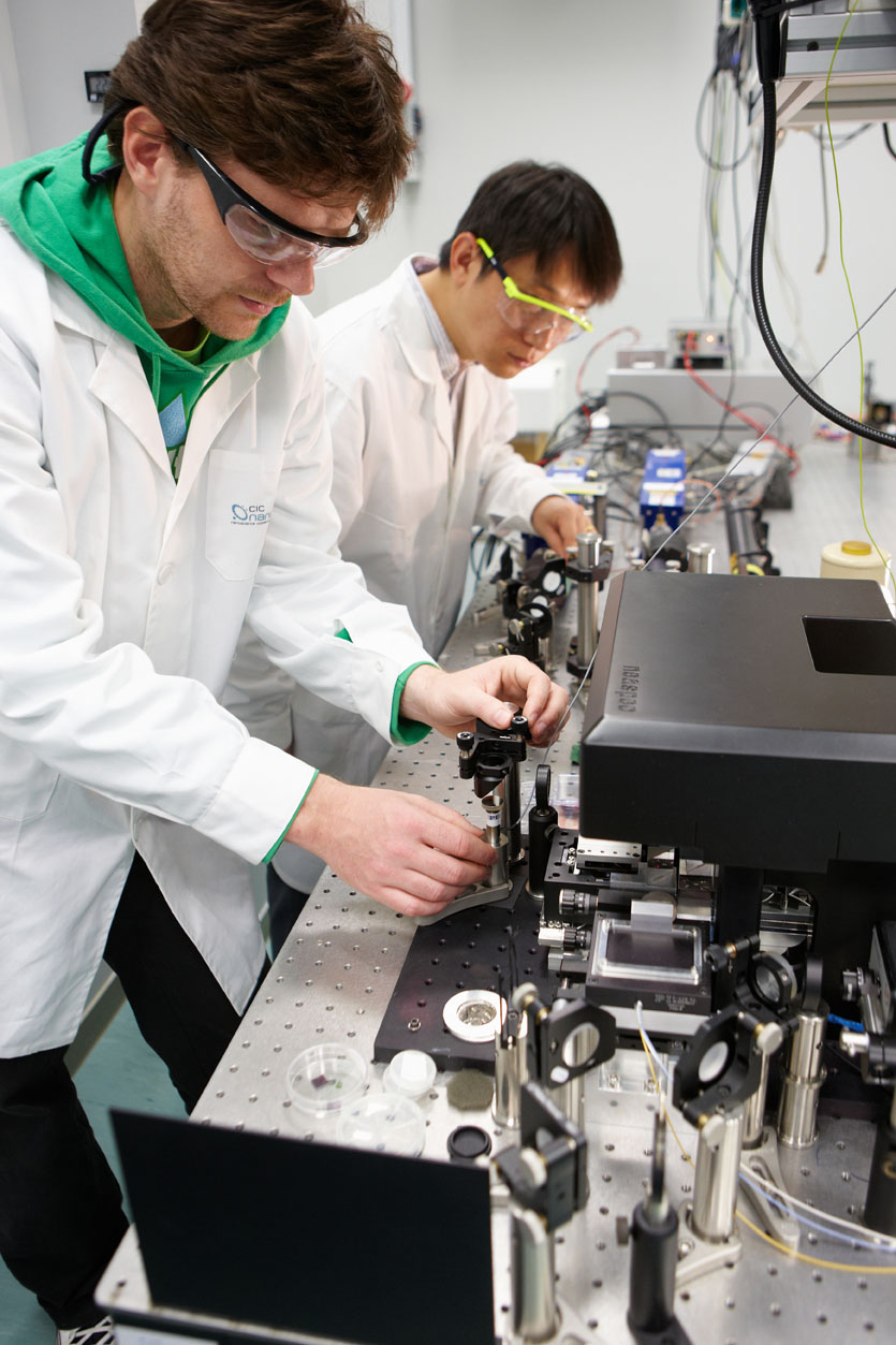
The idea is not new, some physicists have long proposed that plasmons can be created on the surface of graphene. “So far no one has seen the plasmons. They have been indirect measurements, but we and a group from the United States, at the same time, have managed to see the plasmons live,” explains Hillenbrand. They have prepared a microscope called SNOM. “It is unique in the world and we have developed it in our group.” It has been the work of physicists of CICnanoGUNE, since with almost any other type of microscope plasmons cannot be seen.
Hillenbrand wanted to emphasize that it has been a theoretical work. However, it opens the doors for applications: “Now that we know those waves exist, people can believe that and start making the devices they use with those waves.”
Zu idazle
Zientzia aldizkaria